Thin functional Films

Oxidation - PVD - CVD - LPCVD - PECVD - Electroplating

Thin film deposition techniques such as LPCVD, PECVD or PVD are used to coat the surface of a wafer. A variety of materials such as dielectric layers, metal films or poly silicon are available.

This films can be used for their electrical, electrochemical, thermal, piezoelectric, magnetic or mechanical properties. They are usually either selectively deposited (i.e. lift off) or selectively etched away after deposition to form patterned thin films. Commonly deposited layer thickness ranges between nanometers to a few microns.

SILICON OXIDATION

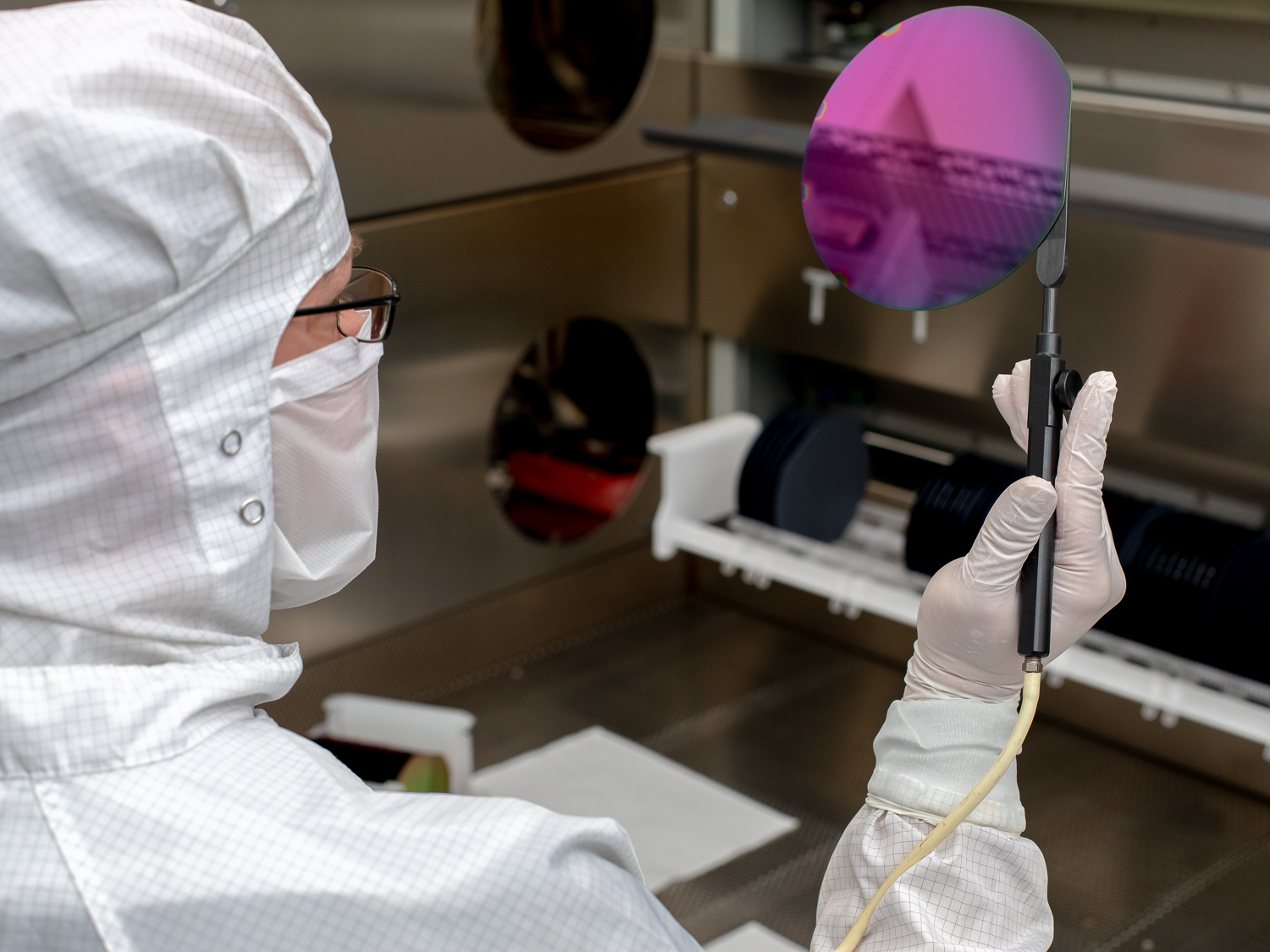
Thermal Oxidation of Silicon
CMOS-compatible quartz furnace processes (Centrotherm), dry and wet oxidation 100 and 150mm wafer size, batch quantity: up to 50 wafers per run.

  • LOCOS oxide (LPCVD nitride mask layer)
  • Gate Oxide, standard thickness 40 nm
  • Field Oxide, standard thickness 1000 nm
  • Cusomized Oxide layers possible, thickness range 10 nm up to 1500 nm
    thickness non-uniformity across wafer: <2%
    average thickness non-uniformity wafer-to-wafer: <3%
    average thickness non-uniformity batch-to-batch: <5%

THIN FILM SPUTTERING

Sputtering

Sputtering as a physical vapor deposition techniques (PVD) used at microfab to form metal and compound/alloy thin films on 100 and 150mm wafer substrates. Two sputter systems (batch coater and a single wafer twin-chamber) are installed and mainly used for deposition of thin metal films for interconnection lines and plating bases.

The following metals are currently available:
Al, AlSiTi, WTi10, W, Au, Pt, Cu, Ti, Cr, Ta

Sputtering of dielectric materials is also possible on the Balzers/Ardenne system by using an rf-source instead of the standard magnetron source. Further, reactive sputtering can be applied for deposition of compound materials such as TiO2, TiN or AlN.

PECVD

Plasma Enhanced Chemical Vapor Deposition (PECVD)

The PECVD technology is used for deposition of dielectric layers at low temperature. Compared to LPCVD where high temperatures of >500°C are needed, this technique can be applied to aluminum metallized wafers, because of the low process temperature of 300°C. Thick layers of up to 5 µm can be deposited using special stress neutralizing processes. PECVD processes are commonly used for metal passivation (“scratch protection and protection from environmental influences”), etch mask generation, sacrificial layer deposition (surface micromachining), mechanical functional layer deposition (membranes, cantilevers). Two multiplex batch systems are currently in operation for PECVD.

LPCVD

Low Pressure Chemical Vapor Deposition (LPCVD)

LPCVD

Centrotherm furnace for up to 150mm wafers.
LPCVD technology is used for uniform, double side deposition of 100 and 150mm size silicon wafers with dielectric or poly-silicon layers at moderate to high process temperatures. Processing is done in three Centrotherm furnaces with 4 tubes each. All applied standard processes are SPC monitored. The layer thickness is measured on test wafers after each run.

Currently available LPCVD thin films

  • TEOS, 100 up to 1200nm, larger thickness possible by multiple depositions and intermediate annael steps
  • Silicon Nitride (stochiometric), 50 up to 200nm, 1.1GPa tensile stress
  • Silicon-rich-Nitride (low stress nitride), 50 up to 800nm, 50 to 180 MPa tensile stress
  • Poly-Silicon undoped, 50 up to 3000nm
  • Poly-Silicon in-situ boron doped, 50 up to 3000nm, resistivity >0.015 Ohm cm

Electroplating

Electroplating for small series

Electroplating with IMI systems
Electroplating of pure metals, such as gold, nickel and copper, as well as alloys of gold and nickel are available for small quantities and R&D batches. This technique is commonly used for microforming applications (filling of high-aspect ratio resist negative forms), e.g. in the fabrication of acceleration sensors or microrelais. As a “cold process”, electroplating is compatible with most CMOS processes, if applied as a back end, post process.

microcoil on top
For example, special MEMS devices such as acceleration senosrs or gyroscopes can be added on top of finished ASIC wafers